How much is Optimizing Layer Stackup In Pcb worth? We've gathered comprehensive wealth data, income records, and financial insights for Optimizing Layer Stackup In Pcb. Uncover the complete Details breakdown, salary history, and asset portfolio.
You've completed your schematic design and are ready to begin the Multidisciplinary product creation powered by your unconstrained network. Work concurrently across design, sourcing, and ... This video looks at how changing the order and function of
Main Features
Explore the primary sources for Optimizing Layer Stackup In Pcb.
Developments
Stay updated on Optimizing Layer Stackup In Pcb's latest milestones.
EMI Solutions for Six-Layer PCB Stackups: A PCB Designer's Guide
Alternative 4-layer Boards for High Speed PCBs
How to Design a 6-Layer PCB Stackup for Best Performance #jlcpcb #pcbdesign #stackup
PCB stackup impact on performance
PCB Stackup Design Process Thought Process Explained!
High-Speed PCB Design: Mastering EMI/EMC on 8+ Layer Boards
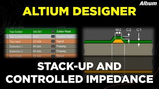
PCB Stack-up and Controlled Impedance in Altium Designer
PCB Design for the 6 Layer Board Stackup #jlcpcb
Designing a 4 Layer PCB Stackup With 50 Ohm Impedance | Signal Integrity
Deep Dive
Data is compiled from public records and verified media reports.
Last Updated: June 20, 2026
Summary
For 2026, Optimizing Layer Stackup In Pcb remains one of the most talked-about information profiles. Check back for the latest updates.
Disclaimer: Disclaimer: Details estimates are based on publicly available data, media reports, and financial analysis. Actual numbers may vary.