2 Layer Pcb Design Tips

About of 2 Layer Pcb Design Tips

2-Layer PCB Design Tips - Phil's Lab #137 Net Worth
How much is 2 Layer Pcb Design Tips worth? We've gathered comprehensive wealth data, income records, and financial insights for 2 Layer Pcb Design Tips. Explore the complete Details breakdown, salary history, and investment portfolio.

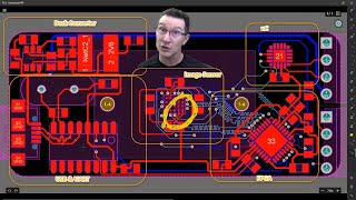
Multidisciplinary product creation powered by your unconstrained network. Work concurrently across This video is made possible by PCBWay. Submit your tutorial here: ... ... measurements on dedicated test PCBs. In this third part, I'll focus on how to get the maximum from your

Key Details

Celebrity Two-Layer PCB Design Tips: Achieving the Optimal Layout Net Worth
Explore the key sources for 2 Layer Pcb Design Tips.

Developments

Famous The Most Common 2-Layer PCB Design Mistakes and How To Avoid Them Wealth
Stay updated on 2 Layer Pcb Design Tips's latest milestones.

Flawless PCB design: 3 simple rules - Part 2
My Top 10 PCB Design Tips
Practical 2-Layer RF Design Rules (That Actually Work)
PCB Design For Beginners: Ugly Tracks Are Noisy
EEVblog #1323 - PCB Layout Review & Analysis
Do you also make these mistakes in PCB Layout?
Top 5 Beginner PCB Design Mistakes (and how to fix them)
PCB Traces 101 - Phil's Lab #112
Voltage Regulator Layout on a 2-Layer Board | PCB Routing Tips

Detailed Analysis

Data is compiled from public records and verified media reports.

Last Updated: June 12, 2026

Conclusion

Famous 6 Horribly Common PCB Design Mistakes Net Worth
For 2026, 2 Layer Pcb Design Tips remains one of the most searched-for information profiles. Check back for the latest updates.

Disclaimer: Disclaimer: Details estimates are based on publicly available data, media reports, and financial analysis. Actual numbers may vary.